
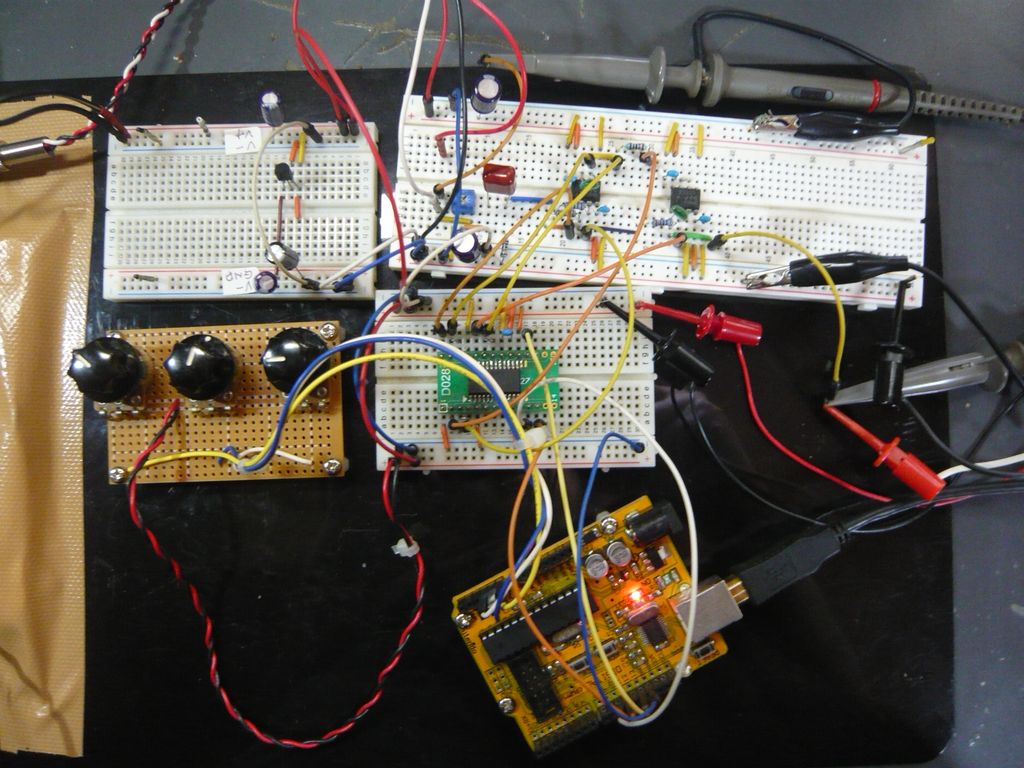
ブレッドボード配線図

Arduinoのスケッチ
<AD8403_SVF_Pot_Control.ino>
/*
  Digital Pot Control

  AD8403

  2つのPOTの出力電圧を読み取って
  Digi-Potのチャンネル1, 2, 3の抵抗値を可変

  Pinの接続
  A0 POT1
  A1 POT2
  10 CS
  11 MOSI
  13 SCK
*/

// inslude the SPI library:
#include <SPI.h>

// set pin 10 as the slave select for the digital pot:
const int slaveSelectPin = 10;

byte cnt;
byte v0, v1;

void setup() {
  // set the slaveSelectPin as an output:
  pinMode (slaveSelectPin, OUTPUT);
  // initialize SPI:
  SPI.begin();
  delay(1);

  Serial.begin(9600);
}

void loop() {
  v0 = analogRead(0) / 4;
  v1 = analogRead(1) / 4;

  Serial.print(v0);
  Serial.print("\t");
  Serial.print(v1);
  Serial.print("\n");

  // Channel2 Q
  digitalPotWrite(1, v0);
  // Channel1, 3 Cutoff
  digitalPotWrite(0, 255 - v1);
  digitalPotWrite(2, 255 - v1);
  delay(1);
}

void digitalPotWrite(int address, int value) {
  // take the SS pin low to select the chip:
  digitalWrite(slaveSelectPin, LOW);
  //  send in the address and value via SPI:
  SPI.transfer(address);
  SPI.transfer(value);
  // take the SS pin high to de-select the chip:
  digitalWrite(slaveSelectPin, HIGH);
}
配線が楽になりそうなので、B端子とW端子(普通のPOTで言う1番と2番)で抵抗値を変化させている。設定値が大きくなると抵抗値が小さくなるので、プログラムで
digitalPotWrite(0, 255 - v1);として反転させている。
digitalPotWrite(2, 255 - v1);
前回の実験と同じく、Qを決めるch2を20kΩ、カットオフ周波数を決めるch1、ch3が15kΩになるように値を設定して波形を見てみた。
DATASHEETの抵抗値を求める計算式
RWB(D) = (D /256) * RAB + RW (RAB = 100kΩ、RW = 50Ω)から、
設定値
ch2: 46: 18018.75Ω + 2.2kΩ ≒ 20.2kΩ※ch2は2.2kΩのゲタを履かせている。
ch1,ch3: 217: 約14.9kΩ
電源電圧(フィルタ回路) -2.47V / +2.54V
電源電圧(Digi-Pot回路) 5.01V
OPAMP NJM2732
LPF

ch1:入力 ch2:LPF出力
BPF

ch1:入力 ch2:BPF出力
HPF

ch1:入力 ch2:HPF出力
入力は単電源波形で、なおかつ試しに入力のGNDをフィルタ回路の仮想GNDではなく、電源のGNDに接続している。どっちがいいのかはよくわかっていない(^q^;
基板図

※配線まだ
部品並べ

C基板でなんとかなるかな?
メモ:
AD8403の余っている1回路とOPAMPの余っている1回路で入力ゲイン調節もできそうだが。
0 件のコメント:
コメントを投稿